EMLs: The Unsung Heroes Powering AI's Digital Arteries
How microscopic semiconductor devices move AI data at light speed through modern data centers

Deepak Shivaprasad
Senior Director of Product Line Management

In the high-stakes world of artificial intelligence and cloud computing, where milliseconds matter and petabytes of data flow continuously, there's a critical technology that rarely makes headlines: the Electro-absorption Modulated Laser, or EML.
Like arteries pumping lifeblood through the human body, EMLs drive optical pathways, moving information at the speed of light between compute nodes, storage systems, and networks. Without optical connectivity, every GPU cluster would sit idle and isolated, every training run would stall, and the AI revolution would grind to a halt. In AI data centers, where speed is everything, these are the unsung heroes making the impossible possible.
Understanding EML Technology
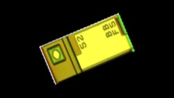
An Electro-absorption Modulated Laser (EML) is a photonic integrated circuit that integrates two key components on a single indium phosphide chip: a Distributed Feedback Laser (DFB) and an Electro-Absorption Modulator (EAM). The DFB generates a stable, wavelength-stabilized optical carrier signal. The EAM then rapidly changes its absorption properties in response to electrical data signals, modulating this continuous-wave light at extraordinary speeds. Modern EMLs routinely support 100 Gbps per lane, with next-generation 200 Gbps per lane designs already in production.
The elegance of EML technology lies in its combination of low chirp (minimal frequency variation enabling longer transmission distances), high extinction ratio (clear distinction between signal states), superior signal fidelity, and energy efficiency. EMLs support advanced modulation formats like four-level Pulse Amplitude Modulation (PAM4), which transmits two bits per symbol, effectively doubling the data rate over the signaling rate. The integration of laser and modulator on a single chip reduces packaging complexity, improves thermal behavior, and enhances reliability.
The Scale of the Challenge: The EML Demand Equation
Understanding the technology is one thing, but grasping the scale at which these components must operate is quite another. The global AI data center market, valued at approximately $15 to $17 billion in 2024, is projected to surge to $60 to $165 billion by 20301 with hyperscalers like Microsoft, Amazon, Google, and Meta collectively investing nearly $200 billion in 20242 alone. To put the infrastructure challenge in perspective: AI-driven data center power capacity in the United States is projected to grow from 30 gigawatts in 2025 to over 90 gigawatts by 2030, exceeding California's entire power demand today3. Training workloads now demand power densities of 100 to 200+ kilowatts per rack, with new systems pushing toward one megawatt per rack3.
This massive power density is mostly due to an equally massive data throughput requirement, and that's precisely where EMLs become indispensable. Most high-speed optical transceivers, the physical interfaces converting electrical data into optical signals and back again, rely on EML laser transmitters for high-speed applications. In a 400G FR4 transceiver, four 100G EMLs operate in parallel, each handling one wavelength in a standardized Coarse Wavelength Division Multiplexing (CWDM4) grid.
The mathematics of scale are clear. Consider a single 51.2 Tbps switch with 64 ports of 800G. Each 800G port can use an optical transceiver containing eight individual 100G EML chips (since 8 x 100G = 800G). Multiply that across all 64 ports, and you get 512 EML chips in just one switch (64 ports x 8 EMLs per port = 512 chips). In a facility with 100 such switches, you need over 51,000 EML chips. Hyperscale AI data centers deploying thousands of switches require millions of EMLs. Industry projections indicate that global demand for 800G+ optical transceiver modules will reach 24 million units in 2025 and surge to nearly 63 million units by 20264, translating to approximately 200 to 500 million EML chips annually.
The speed evolution tells a compelling story. The 400G era, deployed around 2020 to 2022, established 100G PAM4 per lane as the standard. The 800G generation doubles throughput through either an 8x100G architecture or a 4x200G architecture using next-generation 200G EMLs, with shipments surging in 2024 and expected to double again in 20254. The transition to 1.6T is accelerating faster than anticipated5 according to industry analyst LightCounting.
Each speed jump demands more from EML technology: higher bandwidth, lower noise, better extinction ratios, tighter thermal management, and enhanced reliability under stress. Without them, scale-out architectures connecting thousands of GPUs would collapse, data center interconnects would fail, storage networking would bottleneck, and the entire AI infrastructure performance can suffer. In essence, EMLs are the physical embodiment of data center arteries, and if they fail or cannot meet demand, the entire system would be considerably constrained.
When Demand Surge Meets Quality
As data centers transition from 400G to 800G and 1.6T, the margin for error in laser manufacturing vanishes. In this regime, scaling is not merely a matter of increasing volume; it is a matter of maintaining manufacturing excellence at the limits of physics. The "cost of quality" in EML production is exponential. Because these devices are deployed by the millions in synchronized GPU clusters, a single failing EML can cause a "cascading stall." If one laser in an 800G transceiver fails during a multi-week training run involving 50,000 GPUs, the entire computation may need to roll back to the last checkpoint, costing hundreds of thousands of dollars in wasted compute time.
The Reliability Challenges of Advanced Photonics:
- Epitaxial Precision: EMLs require multi-stage epitaxial material growth, where different semiconductor materials are joined with nanometer precision. Any impurity or crystal defect can shorten lifetime.
- Thermal Management at Scale: At 200G per lane, the heat density on the InP chip increases significantly. Control is critical to prevent wavelength shift and extinction-ratio degradation.
- Signal Integrity (PAM4): Unlike traditional, two-level "on-off" signals, PAM4 uses four distinct voltage levels to encode data. This requires the EML to be incredibly linear. Even minor manufacturing variations, tolerable at lower speeds, create "noise" that prevents the DSP (Digital Signal Processor) from recovering data at 1.6T speeds.
- ESD Sensitivity: Integrated EMLs are more ESD sensitive than discrete components. Robust cleanroom protocols and packaging reliability are non-negotiable.
In the AI era, quality is no longer a premium feature; it is an existential requirement. Cisco Systems captures this reality as follows: “each hour of [GPU] downtime due to optics failures could cause a loss of from $2,000 to $12,0006. In other words, quality is not a nice-to-have spec sheet parameter - it is a budget line item.
Lumentum's Edge - Scaling with Quality
When quality becomes existential and volumes reach millions of units annually, the differentiator is straightforward: who can scale optical lanes without trading reliability for volume. Lumentum's edge comes from high-volume indium phosphide-based chip manufacturing, complete vertical integration, and a multi-site footprint designed to support volume ramps while protecting field reliability.
Unlike companies who outsource epitaxial growth, Lumentum controls the entire lifecycle from initial wafer fabrication through final chip packaging. The company operates wafer fabs in San Jose, CA (USA), Caswell (UK), and Sagamihara and Takao (Japan), with flagship assembly and test in Thailand, providing geographic diversification that ensures supply continuity during periods where 800G and 1.6T components face projected supply gaps approaching 40-60%7.
Lumentum’s experience validates and enables execution at scale.
- Over 125 million optical components shipped in the last five years.
- Number one quality score for EMLs from top-tier customers for two consecutive years.
- Lumentum is currently shipping 200 Gbps per lane EMLs at scale, the foundational component enabling the latest 800G & 1.6T transceivers.
- Recent quarters saw record EML revenue, with production capacity expanding 40%8 year over year to meet hyperscaler demand.
- The GaAs platform alone has shipped over 2 billion VCSEL arrays with negligible RMAs, a level of manufacturing maturity now applied to complex InP EMLs powering AI clusters.
Furthermore, stress testing in our Telcordia GR-468 qualification validates field reliability. Industry awards from Lightwave Innovation Reviews9 and ECOC recognize innovation10, but our deeper validation comes from deployment across data center networks globally.
In a market where bandwidth scaling and uptime are inseparable, the advantage isn't merely having a fast EML. It's having a repeatable, customer-audited, high-volume InP manufacturing operation that can ship at scale while holding the reliability line that hyperscale AI demands.
Conclusion
In the high-stakes race for AI supremacy, speed may be the goal, but quality and reliability are an absolute requirement. As the data center "arteries" face unprecedented pressure from the transition to 800G and 1.6T and a global supply crunch, there is no room for a weak link.
Lumentum doesn’t just build EMLs; it builds certainty. By pairing our telecom-grade pedigree with in-house manufacturing, we ensure that these unsung heroes perform flawlessly under stress. When network performance depends on microns of epitaxial material, it matters who builds it - Lumentum can be a partner that meets industry scale without compromising the quality and consistency your links can rely on.
Explore our EML solutions moving AI data at light speed.