
Video
Ask the Expert Video Series: Episode 4 with Matt Sysak
With 400G around the corner, what's needed to enable the next speed node?

AI Infrastructure Is Becoming a Living System The brain may direct the body, but it relies on the heart, blood vessels, and lungs to circulate oxygen, carry signals, and keep every organ in sync. AI infrastructure is reaching a similar point. For several years the industry has focused on compute: GPUs, accelerators, memory, and the race to deliver more tokens at lower cost. That focus was right. But as AI clusters scale from racks to rows to full campuses, compute is no longer the only constraint. The cluster only performs if data can move across it with the bandwidth, latency, power efficiency, and reliability these workloads demand. That movement runs on optical connectivity, which is becoming the circulatory system of AI infrastructure. AI Is Pulling Optics into the Critical Path The capital going into AI infrastructure tells the story. The four largest US hyperscale cloud data center operators are now planning up to $725 billion in 2026 capital expenditures, a 77% increase over their record $410 billion in 20251. When Microsoft, Amazon, Google, and Meta all raise spending at once, the demand signal for everything downstream is hard to miss. The optical market already shows the pull. LightCounting's April 2026 forecast puts Ethernet transceiver growth at 93% in 2024 and an estimated 82% in 2025, with another 65% expected in 2026, and reports demand running 30% to 50% ahead of supply, limited by production capacity for InP EML and laser chips2. Lumentum’s own OFC 2026 investor briefing framed this in InP lane terms: we expect roughly 85% CAGR in InP optical lane volume for EML, CW, and UHP lasers from AI data centers3. The point worth holding onto is that this is a wafer, laser, and chip capacity signal, not only a transceiver one. 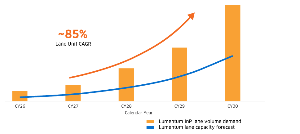 Figure 1. Lumentum OFC 2026 Investor Briefing view of InP optical lane demand from AI data centers, including expected 85% CAGR in InP optical lane volume demand for EML, CW, and UHP lasers3. AI Turns Performance into a System Problem AI workloads push data centers to behave less like collections of servers and more like one large, distributed computer. Scale-up fabrics connect accelerators at very low latency and tight synchronization. Scale-out fabrics hold thousands to millions of endpoints together. Scale-across fabrics reach between buildings, campuses, and metro distances. At the Optica Executive Forum during OFC 2026, OpenAI’s Richard Ho argued that interconnect, memory, and system architecture now matter as much as raw compute, and that optics is the inevitable interconnect once bandwidth density and power per bit become the limiting factors4. Lumentum CEO Michael Hurlston made the same point: “Lumentum’s inclusion in the Nasdaq-100 underscores the critical role our optical products play in AI-driven infrastructure. As the speed and bandwidth inside data centers increase, so does the need for optical solutions”5. Optics is no longer confined to the edge of the network. It is moving deeper into the compute fabric, closer to the switch ASIC and the accelerators, into the places where power, density, and reliability are most constrained. Why the Optical Component Stack Is Broadening The industry will not scale AI on a single optical architecture. Scale-up, scale-out, and scale-across each need different things, and LightCounting's Executive Forum report makes the same point: no single solution covers all three, and a combination of technologies will be required4. The stack is broadening rather than consolidating. EMLs remain essential for the high-speed pluggables used in scale-out networks. CW lasers are the light source for silicon photonics. Ultra-high-power (UHP) lasers and ELSFP architecture grow more important as CPO and NPO move optics closer to the ASIC or GPU. High-speed photodiodes such as LIPD matter more as 200G/lane proliferates and link budgets tighten. On pluggables, EML capacity is the near-term constraint. We have grown EML laser shipments more than 8x from FY20 to FY26E and expect to add more than 50% EML unit capacity by the end of CY26 against CY253. Deployment of 200G/lane and 1.6T optics turn the AI network roadmap directly into high-volume InP laser demand.
 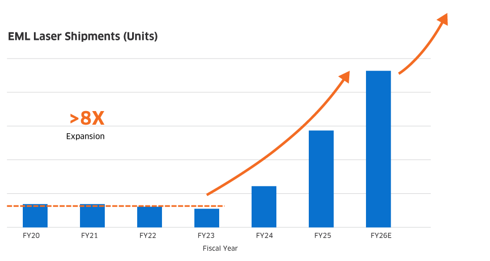 Figure 2. Lumentum OFC 2026 Investor Briefing summary of EML laser shipment expansion and expected EML unit capacity addition by end CY26 versus end CY253. On CPO, the laser source is where much of the system performance is won or lost. In data presented by Lumentum’s CTO Matt Sysak at LightCounting's co-packaged optics conference, our ultra-high-power laser platform is designed to deliver the optical output, efficiency, spectral stability, and low-noise performance required as CPO moves optics closer to the switch ASIC or GPU6. Those numbers matter because CPO is constrained by power, cooling, thermal margin, and long-term link stability as much as by bandwidth.
 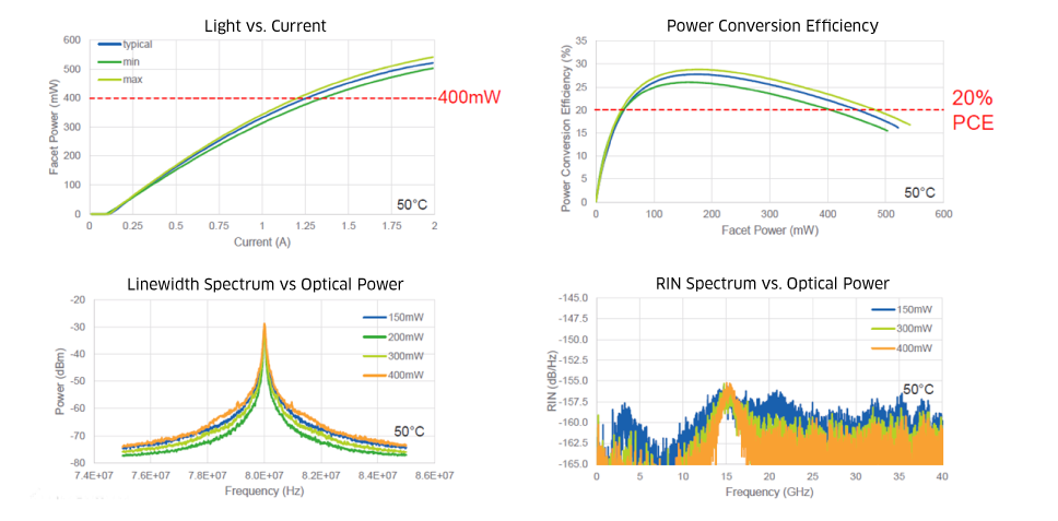 Figure 3. Lumentum UHP laser performance for CPO laser source: light-current output, power conversion efficiency, linewidth spectrum, and relative intensity noise at 50 °C6. Demand appears to back that up. We estimate UHP laser chip units growing at more than 200% CAGR from CY25 to CY30, with initial supply from our San Jose fab and incremental UK fab shipments starting in late summer 2027, and new capacity planned to augment the ramp3. Meeting that is a capacity, manufacturing, and allocation problem, not only a device problem.
 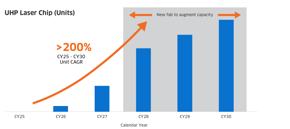 Figure 4. Lumentum OFC 2026 Investor Briefing view of UHP laser chip unit growth and planned capacity expansion to meet CPO demand3. At AI Scale, Stability Becomes an Economic Metric In a traditional network, optical component failure is a service event. In an AI cluster, instability can become a significant infrastructure efficiency problem. When thousands of expensive accelerators are synchronized on a single workload, one weak link drags down useful output, adds recovery overhead, and erodes the return on the whole cluster. As this scales, customers are starting to judge optical components less by peak speed and more by what they contribute to the system: stable links, predictable behavior over temperature, low power per bit, manufacturability, traceability, and long-term reliability. Manufacturing Scale Is the Real Differentiator At AI volumes, the hard part is not the demonstration. It is wafer capacity, process control, yield learning, qualification rigor, traceability, and the ability to ramp complex photonic products repeatably. LightCounting has made the same point: the bottleneck is shifting to back-end manufacturing and supply chain as the industry moves from copper to optics4. We are investing in exactly that. Lumentum builds from the industry's largest InP wafer fab baseline across four fabs, with deep networking heritage, foundational laser technology, and optical switching leadership behind it3. We have also announced a new UHP laser fab in Greensboro, North Carolina, acquired from Qorvo: a 240,000-square-foot facility being retrofitted for 6-inch InP wafer production, with UHP and CW laser ramp expected in mid-2028, up to $5 billion in annual revenue capacity at chip-level margins, and NVIDIA already named as a customer7. Where Lumentum Fits The leading AI players now treat optics as strategic rather than interchangeable. LightCounting describes NVIDIA as building its moat through system design and partnerships, including targeted investments that lock in core manufacturing capacity and strengthen its ecosystem8. Lumentum is part of that picture: we received a $2 billion investment from NVIDIA under a nonexclusive agreement that includes multibillion-dollar purchase commitments and access rights to future production capacity for advanced laser and optical networking products8. We have spent two decades building the InP laser and optical component capability that AI infrastructure now requires, across long-haul networks, data center interconnect, laser chip technology, optical switching, and compound semiconductor manufacturing3. That foundation is what makes this moment concrete for us. The shift to optics-intensive AI infrastructure runs directly through our portfolio: EMLs for high-speed pluggables, CW lasers for silicon photonics, ultra-high-power lasers for CPO and ELSFP, LIPD for high-speed receive, and optical switching for more resilient fabrics. The question for the industry is no longer whether optics will matter at AI scale. It is whether the optical ecosystem can deliver stability, manufacturing discipline, and supply capacity that these workloads demand, and do it repeatably at volume. That is the work our team is focused on, and it is where we intend to lead. Explore additional perspectives on AI infrastructure, technology, and innovation on the Lumentum Blog. References 1) Business Insider, “Big Tech Is Spending up to $725 Billion on AI This Year,” April 2026. Available at: businessinsider.com. 2) LightCounting, Optical Communications Market Forecast, April 2026. 3) Lumentum, Illuminating the Networks of Tomorrow: OFC 2026 Investor Briefing, March 17, 2026. 4) LightCounting, Executive Forum: How AI is Reshaping the Optical Industry, April 7, 2026. 5) Lumentum, “Lumentum Joins the Nasdaq-100 Index, Achieving New Milestone in Global Growth,” May 2026. 6) Matt Sysak, VP, CTO Cloud and Networking, Lumentum, “High Power Lasers for Co-Packaged Optics,” LightCounting Tracking Progress in Co-Packaged Optics Virtual Conference, July 15, 2025. 7) Lumentum, “Lumentum Announces New U.S. Manufacturing Facility to Produce Advanced Lasers for the World’s Largest AI Data Centers,” March 26, 2026. 8) LightCounting, NVIDIA Builds Its Moat Through System Design and Strategic Partnerships, April 16, 2026.
With 400G around the corner, what's needed to enable the next speed node?


